Applications


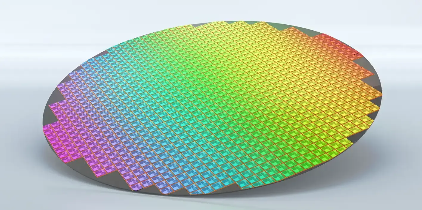
Substrate

ULTRA-THIN GLASS
0.1 ~ 0.3 mm thick
Ø 200 mm

Wafer level optics
3D sensing
WAFER (Si, InP, GaAs)
0.7 mm thick
Ø 4″, 6″, 200/300 mm
Wafer level optics
Laser diodes
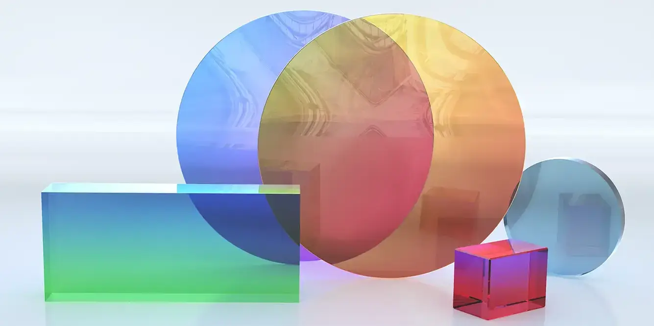
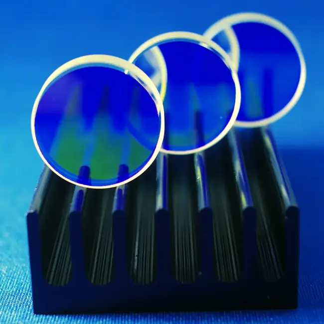
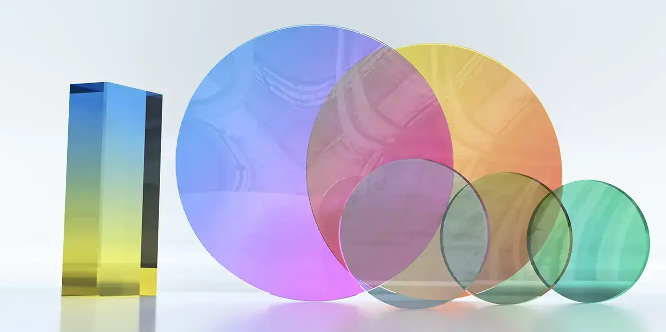
STANDARDS
1.0~6.5 mm thick
Ø1″, 2″, 25/50 mm
□ 50x50/100x100 mm²
Catalog optics
Laser optics
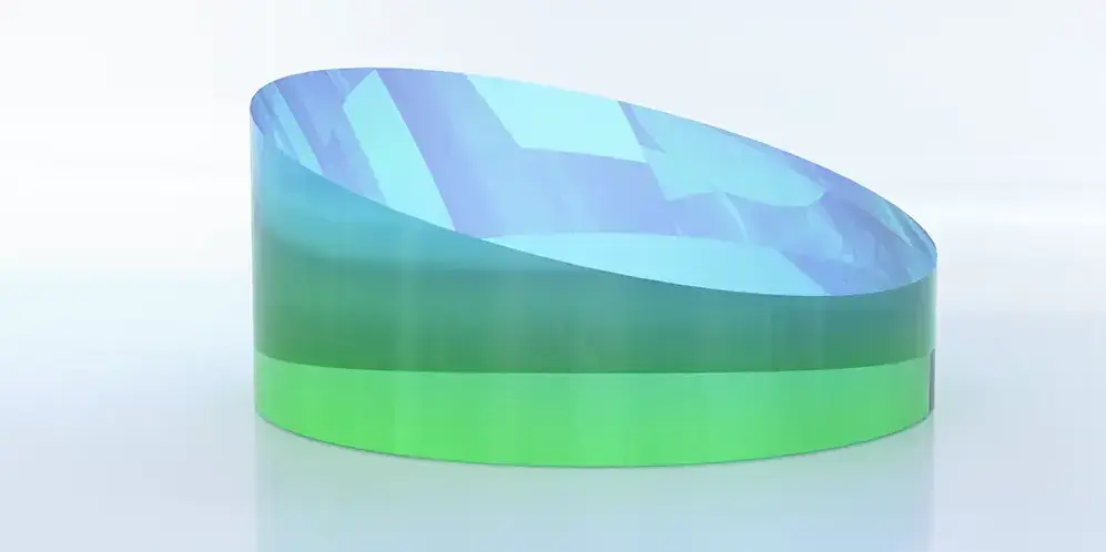
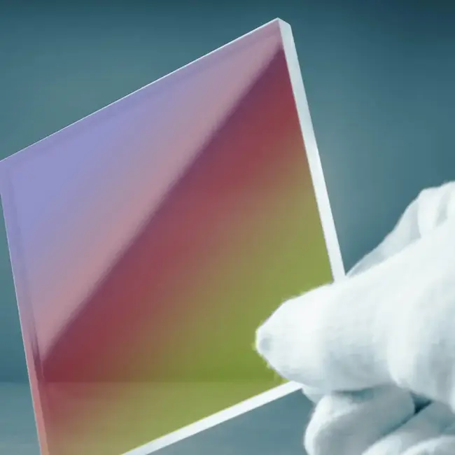
WEDGED-SHAPE
Like standards but with
nonparallel surfaces
(Δ << 1°)
Catalog optics
Laser optics
LARGE AREA
2~50 mm thick
Ø up to 200 mm
□ up to 300x400 mm²
AV/VR/XR
Automotive, HUD
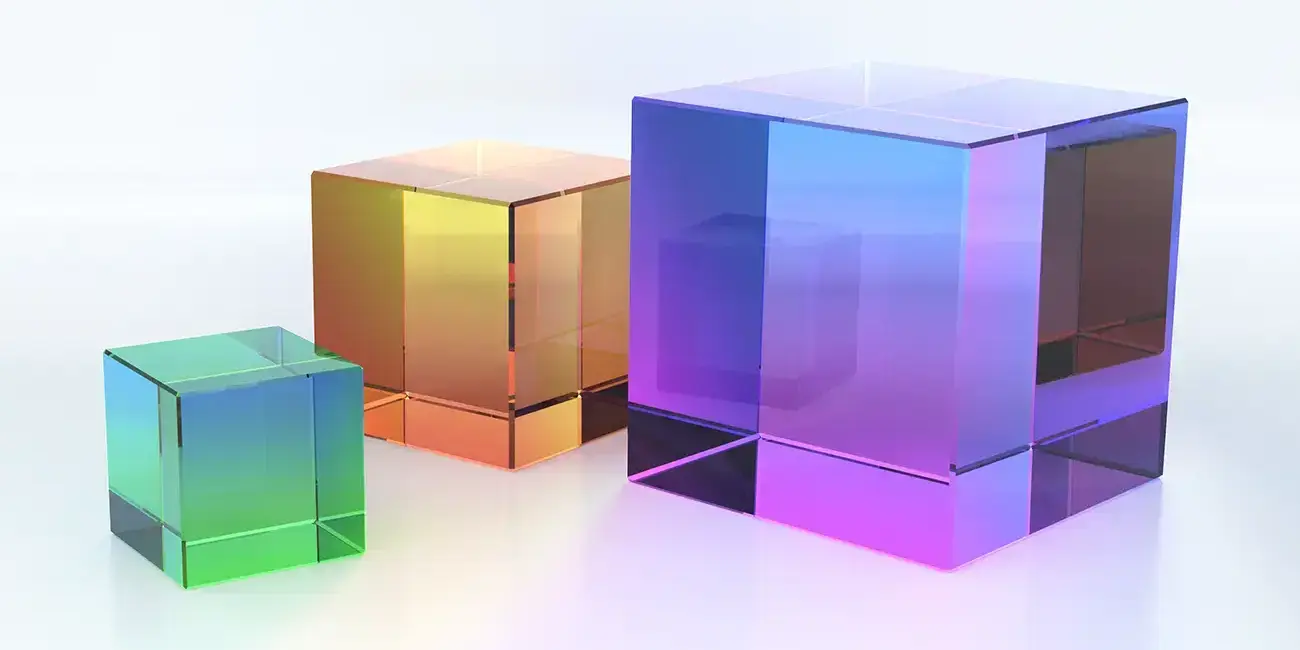
CUBICAL
5x5x5 mm³ up to
70x70x70 mm³
Telecom optics
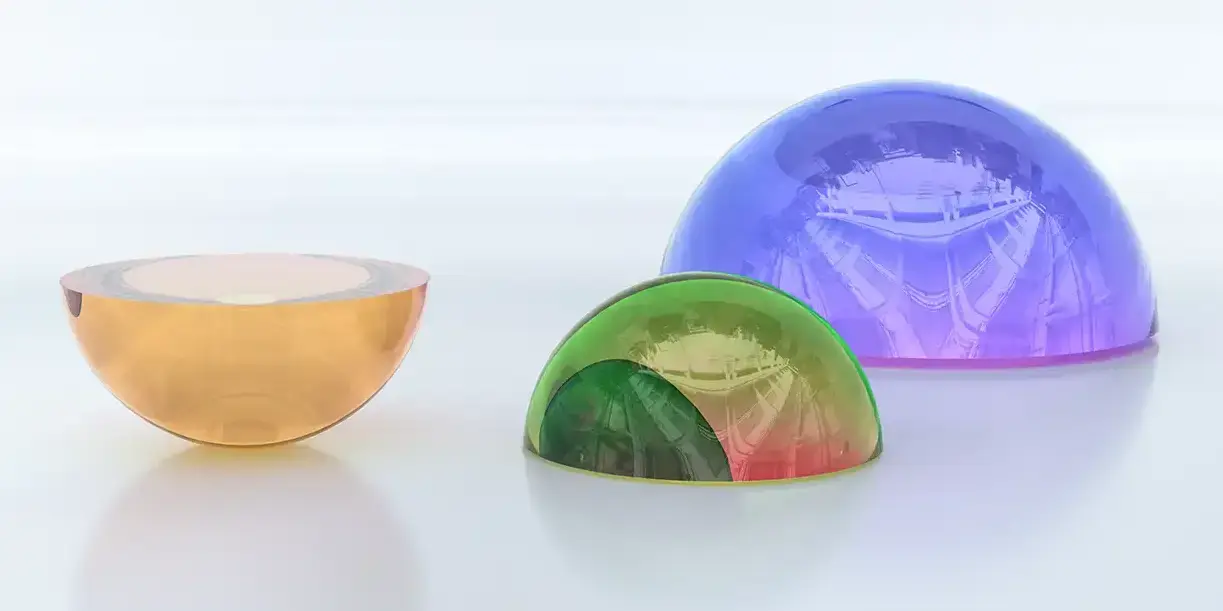
SPHERICAL
5-70 mm thick
Ø up to 200 mm
Laser optics
X-ray/EUV optics
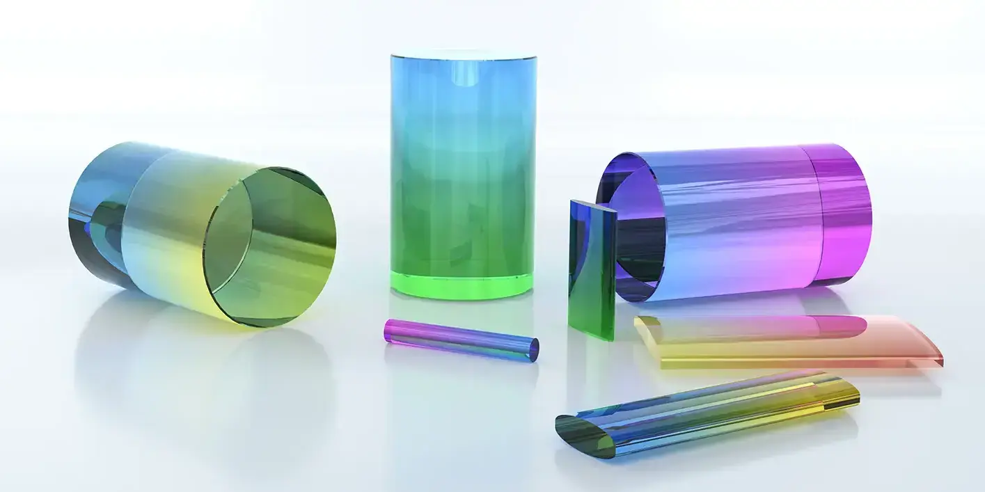
CYLINDRICAL
up to 70 mm thick
up to 200 mm wide
Laser optics
X-ray/EUV optics
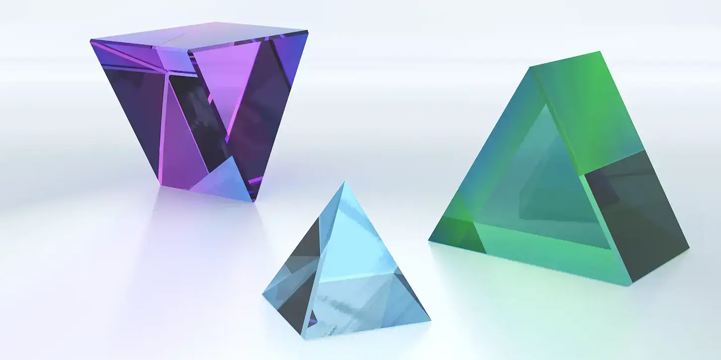
PRISM
Up to 70 mm
edge length
Catalog optics
Periscope optics
Support

Engineering
Simulation . Sampling . Layout
Technology & Application Center
Sampling . Development . Scaling

Service
Customer Portal . Spare Parts . Trainings
CONTACT
20.01.2026 - 22.01.2026
SPIE Photonics West 2026
San Francisco, CA, USA
The Moscone Center
Booth 2261
VON ARDENNE India Pvt. Ltd.
Urban Wrks, 2nd Floor, Koncord Tower, Bund Garden, Sangamvadi, PUNE
411001 MAHARASHTRA
INDIA